ARM describes finfets in the real-world
Finfet technology, with its 3D
structure, is seen as the key semiconductor technology for the next generation
of deep sub-micron chip design. Leah Schuth describes how physical IP
developers will rise to the challenge.
The semiconductor industry faces a
major change in the way that ICs are made in order to keep improving
performance and density – a change that has potential ramifications for design
methodologies. Foundries are preparing to ramp up 14nm and 16nm processes that
use three-dimensional transistor structures based on the finfet concept as they
provide higher performance than can be achieved using the planar transistors of
the 20nm generation.
Raising the channel through which
carriers flow so that the gate can be wrapped around three of its sides means
the gate then exhibits much greater electrostatic control. This overcomes the
short-channel effects that lead to excessive leakage and other problems of
nanometre-scale planar transistors fabricated on bulk-silicon wafers.
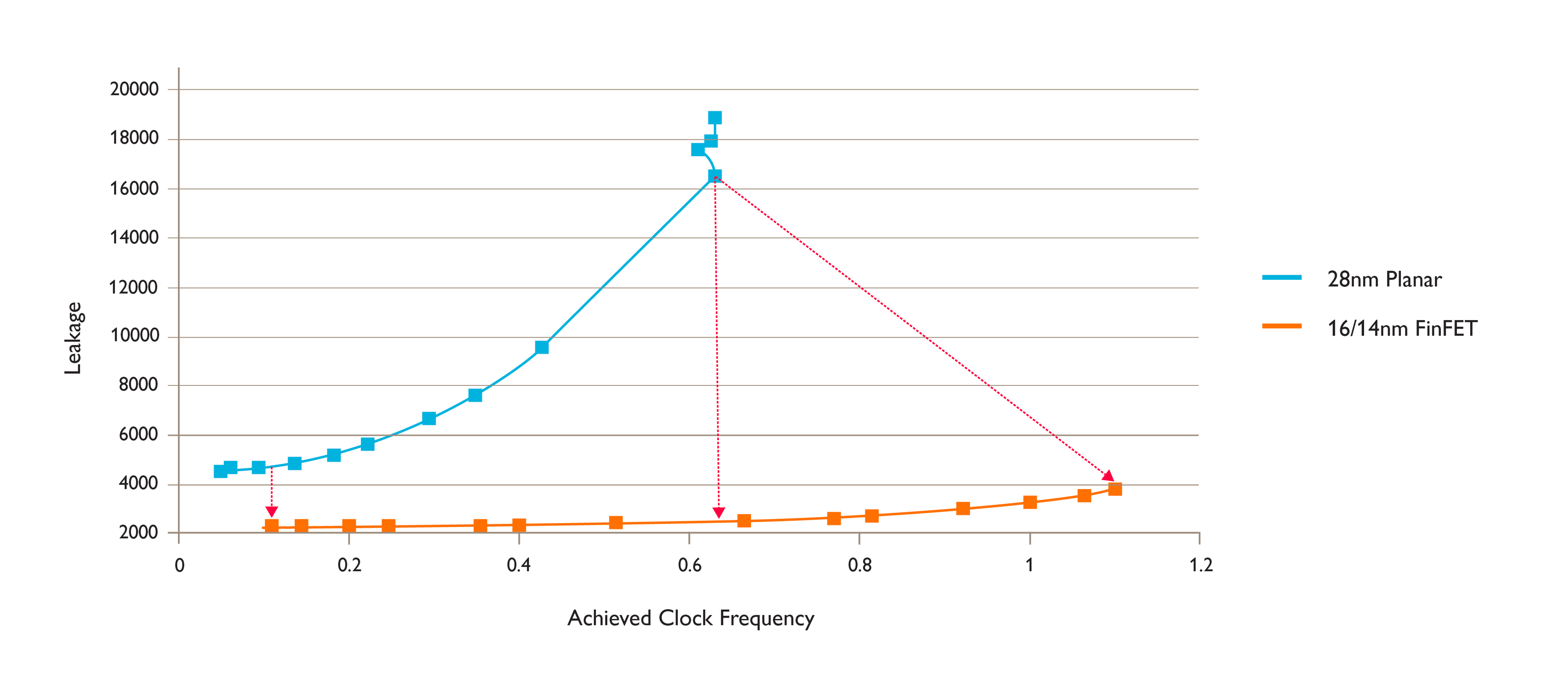
Figure 1: Graph to illustrate
better Leakage Control Across Frequency Range
A further advantage of the multi-sided gate is more drive current
per unit area than planar devices – the height of the fin can be used to create
a channel with a larger effective volume than a planar device with the same
equivalent gate length. This translates into better effective performance.
The added performance capability of finfets can be used to achieve
higher frequency numbers compared to bulk for a given power budget. The power
reduction can come from two sources: reduced need for wide, high-drive standard
cells; and the ability to operate with a lower supply voltage for a given
amount of leakage. But changes to design techniques will be needed to enable
this performance to be fully realised.
Standard cell-based flows remain key to high-productivity IC
implementation. The cell abstraction has underpinned the synthesis-driven flow
for several decades, providing the basis for highly automated digital circuit
implementation that allows comparatively small teams to manage multi-million
gate designs. Changes to the transistor structure and their associated
layout-dependent effects threaten to break through the clean interfaces between
the physical, cell and logical layers of the design process, forcing designers
to take into account low-level features when laying out circuitry. However, by
bringing more intelligence to the cell level, it is possible to maintain the
productivity advantages of the standard cell abstraction and still tease out
the power, performance and area (PPA) advantages promised by finfet-based
processes.
The finfet brings with it some fundamental changes to circuit
structure that are driven by its physical form (Figure 2).The fins on a given
process have a fixed width and pitch. In contrast to planar processes where
transistors can be made wider by arbitrary amounts to improve their overall
drive strength and to improve their performance with large fanouts or
high-capacitance buses, a finfet’s effective width can only be changed by
adding more fins to the transistor. As well as increasing the complexity of
analogue and custom circuit design, fin quantisation has subtle but important
ramifications for digital circuit implementation.
In general, finfet-based processes benefit from as narrow a fin
pitch as possible as this provides better density, flexibility and performance.
The processes used to create the fins rely on chemical self-alignment
techniques that can yield pitches 25 per cent smaller than the pitch of lines
on the finest layers of metal interconnect, M1 and M2. These metal layers are
currently drawn using two independent masks that are overlaid into one
composite exposure rather than using self-aligned processes. The minimum pitch
of these metal layers is determined by the overlay error, resulting in a higher
pitch than can be achieved for the self-aligned fin-formation steps.
The mismatch in fin and M2 pitch – which conventionally runs
parallel to the fins – needs to be factored into the design of standard cells
used to implement the bulk of the digital logic that will be used in a
finfet-based IC.
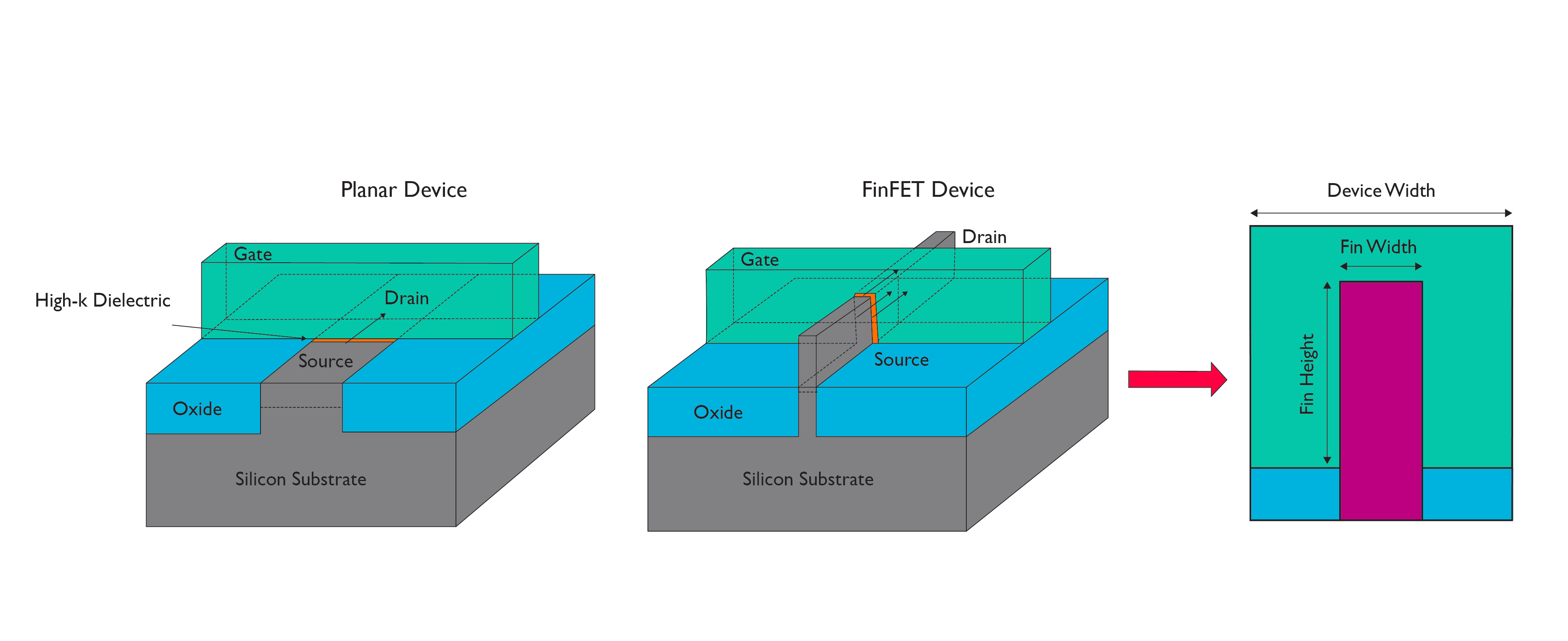
Figure 2: Finfet vs Planar
In the case of finfet -based processes, there are only a few valid
‘gear ratios’ between fin and metal pitches that can result in viable
standard-cell libraries, which need to be designed to fit each of their cells
into a fixed number of tracks. Even then, some combinations will result in
inflexible metal grids that make it difficult to carry sufficient current to
cells on critical paths. Nanometre processes are increasingly prone to effects
such as electromigration that will reduce the lifetime of the IC by gradually
thinning out wires subject to high currents until they break.
For maximum metal wiring density, double-patterning rules enforce
not only the pitch of metal traces but their width. As a result is not always
possible to draw wider metal traces to carry the large currents needed for
cells that provide a high drive. Some ratios of fin count to metal trace count
do allow for more flexible use of metal interconnect for power routing.
These enable the use of wider, more resilient power rails where
they are needed, alongside tracks of cells able to trade higher logic routing
density for power delivery. To be able to take advantage of these structures
calls for a much deeper understanding of standard-cell architecture than is
usually the case in conventional place-and-route tools, which are designed to
treat standard cells as black boxes with a set of I/O and power pins in predetermined
locations.
Tools that are able to use their understanding of the internal
standard-cell architecture and remap cells according to the needs of the logic
can provide the additional flexibility required to make full use of these new
structures without demanding a thorough retooling of the IC-implementation
flow. The same understanding can aid other parts of the flow, through to late
changes in design that result in engineering change orders (ECO).
Because design rules are more restrictive than in the past,
implementing ECOs has become more difficult to perform as even a small change
can lead to issues with mask colouring on double-patterned layers. A flow that
incorporates tools able to comprehend the local standard-cell environment can
manipulate the design at a deeper level to allow ECOs to be implemented as
transparently as possible.
Greater understanding of the internal architecture of standard
cells will help with other issues raised by the migration to nanometre
processes based on finfets. As designers attempt to take advantage of the
higher performance of the 3D transistors and push up clock speeds, they will
encounter tougher variability challenges. Although finfets demonstrate lower
variation than planar transistors for some key metrics, variability remains a
major obstacle to timing signoff and is exhibited in a number of ways that
cross the boundary between standard cells and the routing layer.
Traditionally, such variations would be incorporated into guard
bands that limit clock speed, limiting the performance gains that can be
achieved with the finfet structure. Better analysis and correction techniques
can recover much of this performance loss, leading to higher clock speeds and
products that are more competitive in the market.
The double-patterning techniques employed in the 14nm and 16nm
generation of finfet -based processes have been shown to lead to significant
variations in path delay. For example, a small shift in the alignment of one of
the two masks used to image the interconnect patterns can increase the coupling
capacitance between the gate electrode and the wiring, leading to an increase
in path delay.
Because the shift will be consistent across the entire mask, the
delay for transistors linked by the pattern on that mask will be correlated –
something that can be taken into account by more advanced analysis tools that
have an understanding of the behaviour and internal connections of each
standard cell. By taking these correlations into account and taking corrective
measures, the pessimism introduced by coupling capacitance variation can be
removed and target clock speeds increased.
Interconnect parasitics, particularly the high resistance of metal
traces in finfet-based processes, also limit the performance of clock tree,
which use a large number of long-distance connections to provide consistent
timing across the IC. Traditional techniques such as buffer insertion increase
power consumption. By employing knowledge about the underlying standard cells
it is possible to perform more intelligent clock-tree optimisation and provide
low-skew timing signals without eating into the power budget.
The decrease in device geometries is also leading to increases in
the probability of single-event upsets caused by ionising radiation that lead
to incorrect results and system crashes. Analysis of the structure of cells in
their circuit context, potentially replacing them with hardened versions, can
reduce the probability of improper behaviour in the event of alpha particles.
The move to finfet-based processes brings about a number of
process-level changes that have ramifications for digital design that if not
addressed can lead to poor IC performance. Although these physical effects
potentially threaten the highly stable standard cell-based flow, the
introduction of tools to address SoC design at the cell level will help
maintain the stability of the flow and enable the full performance of
finFET-based processes to be realised.
Writer is Leah Schuth, manager technical marketing, physical
design at ARM
- See more at:
http://www.electronicsweekly.com/news/research/process-rd/arm-describes-finfets-real-world-2014-10/#sthash.0dfMrbzd.dpuf
No comments:
Post a Comment