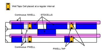
Well
taps (Tap Cells): They are traditionally used so that Vdd
or GND are connected to substrate or n-well respectively. This is to help tie
Vdd and GND which results in lesser drift and prevention from latchup.
End
cap Cells: The library cells do not have cell connectivity as
they are only connected to power and ground rails, thus to ensure that gaps do
not occur between well and implant layer and to prevent the DRC violations by
satisfying well tie-off requirements for core rows we use end-cap cells.
Decap Cells:
They are temporary capacitors which are added in the design between power and
ground rails to counter the functional failure due to dynamic IR drop. Dynamic
IR Drop happens at the active edge of the clock at which a high current is
drawn from the power grid for a small duration. If power source is far from a
flop the chances are there that flop can go into metastable state. To overcome
decaps are added, when current requirement is high this decaps discharge and
provide boost to the power grid.
decap cell.
Tie Cells:
Tie-high and Tie-Low cells are used to connect the gate of the transistor to
either power or ground. In Lower technology nodes, if the gate is connected to
power/ground the transistor might be turned on/off due to power or ground
bounce. These cells are part of standard-cell library. The cells which require
Vdd (Typically constant signals tied to 1) connect to Tie high cells The cells
which require Vss/Gnd (Typically constant signals tied to 0) connect to Tie Low
cells.

Filler
cells: Filler cells are used to establish the continuity
of the N- well and the implant layers on the standard cell rows, some of the
small cells also don’t have the bulk connection (substrate connection) because
of their small size (thin cells). In those cases, the abutment of cells through
inserting filler cells can connect those substrates of small cells to the
power/ground nets. i.e. those thin cells can use the bulk connection of the
other cells (this is one of the reason why you get standalone LVS check failed
on some cells).

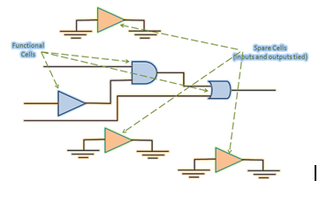
Spare
cells: These are just that. They are extra cells placed
in your layout in anticipation of a future ECO. When I say future, I mean after
you taped out and got your silicon back. After silicon tests complete, it might
become necessary to have some changes to the design. There might be a bug, or a
very easy feature that will make the chip more valuable. This is where you try
to use the existing “spare” cells in your design to incorporate the design change.
For example, if you need a logic change that requires addition of an AND cell,
you can use an existing spare AND to make this change. This way, you are
ensuring that the base layer masks need no regeneration. The metal connections
have changed, and hence only metal masks are regenerated for the next
fabrication.
Kinds
of spare cells: There are many variants of spare cells
in the design. Designs are full of spare inverters, buffers, nand, nor and
specially designed configurable spare cells.
Inserting
Spare Cells
Spare cells need to
added while the initial implementation. There are two ways to do this.
The designer adds separate modules with
the required cells. You start your PnR with spare cells included, and must make
sure that the tool hasn't optimized them away. There can be more than one such
spare modules, and they will be typically named spare* or some such
combination. The inputs are tied to power or ground nets, as floating gates shouldn't be allowed in the layout. The outputs are left unconnected.
Spare
cells can also be added to design by including cells in Netlist itself.