Friday, 18 September 2015

GLANCE ON PHYSICAL VERIFICATION

At Nanometer era of chipdesign physical verification is palying an important role in gainig the attention of the Engineer. as the design shrinks a bunch of new Design Rules rules are creating by the manufacturers  for better productivity and yield of the Chip.

The Main steps in PhysicalVerification includes 
DRC: Design Rule Checks
LVS : Layout Vs Schematic
ERC : Electric Rulr Check


Design Rule Checks: 
  It verifies whether the designed layout can be manufactured by the fabrication lab with a good yield. Here we look after the Physical Design Rule Violations (DRC), the main errors here we see are Min Spacing Violation between same Metal layer,  Minimum area violation, Min width Violation,  Notch violations, Via Enclosure.

Inputs for DRC at Signoff Stage: 
Design Layout (GDSII) 
Design Rule File provided by the fab.

Tools Used for SignOff  DRC: Calibre from Mentor Graphics, Assura From Cadence , Hercules From Synopsys.


Layout Vs SCHEMATIC:

LVS is also an important step in Physical Verification, Here we will verifty that the Design Layout (GDSII) is same as the Netlist (Functionality).

Inputs for LVS:
LVS Rule  File
Circuit Level Design Netlist along with IP (lvs Netlist).
GDSII

LVS is mainly caonsists of 2 steps Extraction and Comparision.

Here First the Design Netlist is converted to circuit level transistors, Diodes, Resistors, Capacitors. then GDS is also converted to its transistor level by extracting These devices are identified in the GDS file by recognition of the layers and shapes that makes up the circuit or by the cell definition of the devices/circuits provided in the cell definition file of the intellectual property blocks or in the LVS rule deck itself, This Process is called Extraction.

Here mainly we can see Power (VDD VSS) Connectivity Errors.

Second stage is comparision Stage after extracting each cell and Net is assigned with a unique Name and Number respectively in GDS and Netlist, with this unique Nubers and names tool will compare all  cells and Nets and throws an Error if any Mismatch occurs.

The Main LVS Erros we observe are 
Incorrect Instances.(Missing Instances).
Incorrect Nets (Shorts, Opens).


Tools Used for LVS: Calibre from Mentor Graphics.
Saturday, 28 February 2015

Multi mode multi corner analysis


Multi mode multi corner analysis

 Introduction to MCMM:
Multi-mode multi-corner (MMMC) analysis refers to performing STA across multiple operating modes, PVT corners and parasitic interconnect corners at the same time. For example, consider a DUA that has four operating modes (Normal, Sleep, Scan shift, Jtag), and is being analyzed at three PVT corners (WCS, BCF, WCL) and three parasitic interconnect corners (Typical, Min C, Min RC) as shown in Table 3.1


Pvt corner/ Parasitic corners
WCS
BCF
WCL
Typical
1: Normal/sleep/scan shift/Jtag
2 :Normal/sleep/scan shift
3:Normal/sleep
Min C
4: not required
5:Normal/sleep
6: not required
Min RC
7: not required
8:Normal/sleep
9: not required
Table 3.1: possible scenarios

There are a total of thirty six possible scenarios at which all timing checks, such as setup, hold, slew, and clock gating checks can be performed. Running STA for all thirty six scenarios at the same time can be prohibitive in terms of runtime depending upon the size of the design. It is possible that a scenario may not be necessary as it may be included within another scenario, or a scenario may not be required. For example, the designer may determine
that scenarios 4, 6, 7 and 9 are not relevant and thus are not required. Also, it may not be necessary to run all modes in one corner, such as Scan shift or Jtag modes may not be needed in scenario 5. STA could be run on a single scenario or on multiple scenarios concurrently if multi-mode multicorner capability is available.

What is the difference between the single, bc_wc, and on_chip_variation analysis modes?


What is the difference between the singlebc_wc, and on_chip_variation analysis modes?
Answer:
This article covers the differences between the singlebc_wc, and on_chip_variation analysis modes in PrimeTime. It will also explain how these three analysis modes are affected by the chosen slew propagation mode (worst_slew or worst_arrival).
The following topics are discussed:
·       Two slew propagation modes
·       Timing paths and their proper analysis
·       Three timing analysis modes
·       Potential for optimism in the single and bc_wc analysis modes

It is important to note that DesignTime's min/max mode refers to min and max corners. Hold paths are only checked at the min corner, but on-chip variation within the min corner is included in the analysis. Likewise, setup paths are only checked at the max corner, but on-chip variation within the max corner is included in the analysis.
The three analysis modes can be summarized in the following two charts:
analysis mode
setup launch path
setup capture path
single
slowest path through max-delay arcs,
single operating condition,
no derating
fastest path through max-delay arcs,
single operating condition,
no derating
bc_wc
slowest path through max-delay arcs,
worst-case operating condition,
late derating
fastest path through max-delay arcs,
worst-case operating condition,
early derating
on_chip_variation
slowest path through max-delay arcs,
worst-case operating condition,
late derating
fastest path through min-delay arcs,
best-case operating condition,
early derating
Table 1: Timing Parameters Used For Setup Checks
analysis mode
hold launch path
hold capture path
single
fastest path through max-delay arcs,
single operating condition,
no derating
slowest path through max-delay arcs,
single operating condition,
no derating
bc_wc
fastest path through min-delay arcs,
best-case operating condition,
early derating
slowest path through min-delay arcs,
best-case operating condition,
late derating
on_chip_variation
fastest path through min-delay arcs,
best-case operating condition,
early derating
slowest path through max-delay arcs,
worst-case operating condition,
late derating
Table 2: Timing Parameters Used For Hold Checks

Monday, 19 January 2015

CONGESTION CONTROL TECHNIQUES


Congestion needs to be analyzed after placement and the routing results depend on how congested your design is. Routing congestion may be localized. Some of the things that you can do to make sure routing is hassle free are:

Placement blockages: The utilization constraint is not a hard rule, and if you want to specifically avoid placement in certain areas, use placement blockages.
Soft blockages (buffer only)
Hard blockages (No std cells and buffers are allowed to Place)
Partial blockages (same as density screens)
Halo (same as Hard blockage but blockage can also be moved w.r.t Macro.)

Macro-padding: Macro padding or placement halos around the macros are placement blockages around the edge of the macros. This makes sure that no standard cells are placed near the pin outs of the macros, thereby giving extra breathing space for the macro pin connections to standard cells.

Cell padding: Cell Padding refers to placement clearance applied to std cells in PnR tools. This is typically done to ease placement congestion or reserve some space for future use down the flow.
For example typically people apply cell padding to the buffers/inverters used to build clock tree, so that space is reserved to insert DECAP cells near them after CTS.

Maximum Utilization constraint (density screens): Some tools let you specify maximum core utilization numbers for specific regions. If any region has routing congestion, utilization there can be reduced, thus freeing up more area for routing.

set_congestion_options -max_util 0.6-coordinate{837 114 1103 918}

DIFFERENT TYPES OF CELLS IN VLSI


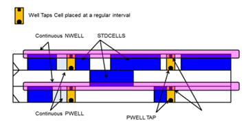
Well taps (Tap Cells): They are traditionally used so that Vdd or GND are connected to substrate or n-well respectively. This is to help tie Vdd and GND which results in lesser drift and prevention from latchup.


End cap Cells: The library cells do not have cell connectivity as they are only connected to power and ground rails, thus to ensure that gaps do not occur between well and implant layer and to prevent the DRC violations by satisfying well tie-off requirements for core rows we use end-cap cells.


Decap Cells: They are temporary capacitors which are added in the design between power and ground rails to counter the functional failure due to dynamic IR drop. Dynamic IR Drop happens at the active edge of the clock at which a high current is drawn from the power grid for a small duration. If power source is far from a flop the chances are there that flop can go into metastable state. To overcome decaps are added, when current requirement is high this decaps discharge and provide boost to the power grid.

decap cell.

Tie Cells: Tie-high and Tie-Low cells are used to connect the gate of the transistor to either power or ground. In Lower technology nodes, if the gate is connected to power/ground the transistor might be turned on/off due to power or ground bounce. These cells are part of standard-cell library. The cells which require Vdd (Typically constant signals tied to 1) connect to Tie high cells The cells which require Vss/Gnd (Typically constant signals tied to 0) connect to Tie Low cells.


 Filler cells: Filler cells are used to establish the continuity of the N- well and the implant layers on the standard cell rows, some of the small cells also don’t have the bulk connection (substrate connection) because of their small size (thin cells). In those cases, the abutment of cells through inserting filler cells can connect those substrates of small cells to the power/ground nets. i.e. those thin cells can use the bulk connection of the other cells (this is one of the reason why you get standalone LVS check failed on some cells).


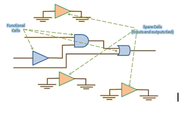
Spare cells: These are just that. They are extra cells placed in your layout in anticipation of a future ECO. When I say future, I mean after you taped out and got your silicon back. After silicon tests complete, it might become necessary to have some changes to the design. There might be a bug, or a very easy feature that will make the chip more valuable. This is where you try to use the existing “spare” cells in your design to incorporate the design change. For example, if you need a logic change that requires addition of an AND cell, you can use an existing spare AND to make this change. This way, you are ensuring that the base layer masks need no regeneration. The metal connections have changed, and hence only metal masks are regenerated for the next fabrication.
Kinds of spare cells: There are many variants of spare cells in the design. Designs are full of spare inverters, buffers, nand, nor and specially designed configurable spare cells.


Inserting Spare Cells
Spare cells need to added while the initial implementation. There are two ways to do this.
                 The designer adds separate modules with the required cells. You start your PnR with spare cells included, and must make sure that the tool hasn't optimized them away. There can be more than one such spare modules, and they will be typically named spare* or some such combination. The inputs are tied to power or ground nets, as floating gates shouldn't be allowed in the layout. The outputs are left unconnected. 

            Spare cells can also be added to design by including cells in Netlist itself.