Showing posts with label FINFETS. Show all posts

Thursday, 18 December 2014

Rectangular FINS VS Triangular FINS


On 23th April Chipworks posted a blog revealing the inner workings of the Intel 22 nm technology and the architecture of the corresponding FinFETs or, as Intel calls them, tri-gate transistors.
Figs 5, 6 and 7 in the Chipworks posting compare the “unexpected” slope of the fabricated transistors with the original tri-gate schematic shown by Intel last year. There is a lot of speculation about the possible advantages and disadvantages of the trapezoidal (or almost triangular) shaped ‘bulk’ FinFET.
Driven by natural curiosity we decided to shine some light on these questions by doing 3D simulations with our ‘atomisic’ simulatorGARAND, although at this initial stage the ‘atomicity’ doesn’t play any role in our simulations. Fig 1 compares the TEM image of one of the FinFETs from Fig. 7 of the Chipworks posting with our simulation domain. Since we do not have information about the doping distribution in the Intel FinFETs we have assumed a lightly doped channel, which is beneficial from the point of view of statistical variability.

intel-fin.giffinfet-structure.png
Fig. 1 Comparison of the TEM image of one of the FinFETs from Fig. 6 of the Chipworks blog with the GARAND simulation domain.

The electron concentration and the potential distribution along the fin are illustrated in Fig.2. We have assumed that there is a high doping concentration stopper below the fin in the STI region. Clearly FinFETs are more complicated devices in terms of understanding and visualisation compared to the ‘old’ bulk MOSFETs.


Electron ConcentrationElectrostatic Potential
Fig. 2 Electron concentration and the potential distribution along the fin.

The current density distribution across the fin in the middle of the channel at different gate bias conditions is illustrated in Fig. 3 and is rather complex. At low gate voltage the maximum current density is in the middle of the channel where the gate has least control over the turning-off of the device. The depletion region caused by the highly-doped stopper below the channel prevents current flow at the very bottom of the channel – one drawback of the bulk FinFET architecture. At high gate voltage the current moves towards the interface, crowding at the top of the fin due to the focusing gate fringing field there, with quantum mechanical confinement concentrating the charge in a small circular region. Fig. 4 animates the changing gate bias, focussing on the fin channel.


Current density with increasing gate voltage
Fig. 3 Current density distribution across the Fin at different gate bias conditions.
Animation of the current density
Fig. 4. Close-up view of the fin with an animation of the current density with increasing gate bias.


Undoubtedly the result that we found most interesting is the comparison in Fig. 5 between the gate length dependence of the threshold voltage for the trapezoidal Intel transistor and an equivalent rectangular-fin transistor (same fin height and with fin width equal to the average width of the trapezoidal fin). Clearly the rectangular fin has better short channel effects. Still, the million dollar question is if the almost-triangular shape is ‘on purpose’ design, or is this what bulk FinFET technology can achieve in terms of the fin etching?


Vt Roll-off
Fig. 5 Threshold voltage dependence on gate length comparing the Intel-type structure with an ideal rectangular FinFET.


We would be delighted to hear your opinions on this interesting device, particularly with regard to the shape.

Wednesday, 17 December 2014

FINFETS

WHY FINFETS


                                        Since the advent of semiconductors and throughout the long history of designing integrated circuits for everything from computer hardware to multifunction mobile devices, the basic tenet of Moore's law has remained the same: the number of transistors on a given area of silicon doubles every two years.
Between the foundries developing advanced process nodes and their consumers' insatiable demand for more functionality, the industry has fulfilled Moore's Law. The transistor count on today's advanced multicore processors is reaching the 3billion range – a long way from the 6800 processor of the mid 1970s that had just 5000 transistors.

Semiconductor manufacturing foundries helped make this growth achievable by introducing smaller geometry cmos process nodes using planar field effect transistor (FET) technology, where the latest node effectively doubled the gate density compared to the previous generation every couple of years. As we approached the sub nanometre range with the 90nm node and beyond, static leakage became an important factor such that while every new process generation may have doubled the gate density, it also doubled the amount of leakage current.

This leakage could be mitigated through the use of high voltage threshold dopants at the expense of device performance, or through the use of advanced design techniques, such as power gating or multivoltage islands. Controlling current leakage when the transistors are switched off is important to preserve battery life or minimise power consumption in computer and mobile applications that spend most of their time in an idle state.

Economics also plays a factor in determining whether to move to advanced processes and when. If chips can take advantage of the increased density to provide more functionality, then it generally made sense to move to the next node, even if mask and process costs were higher. This was the case as designs moved from 65nm to 45/40nm and then again to 28nm. However, the 20nm process node has introduced a new set of challenges, including double patterning and very leaky transistors due to short channel effects. Both are negating the benefits of transistor scaling.

The move from 28nm to 20nm was also unattractive economically for many, since it didn't provide the same level of performance and area gains seen with previous generations. Even with the 30 to 50% density improvement enabled by moving from the 28nm to 20nm process technologies, the performance gain is nowhere near the same as that seen with the move from the 45/40nm to the 28nm process node.

While the planar FET may have reached the end of its scalable lifespan, the semiconductor industry has found an alternative approach with FinFETs; viewed by many as the best choice for next generation advanced processes.

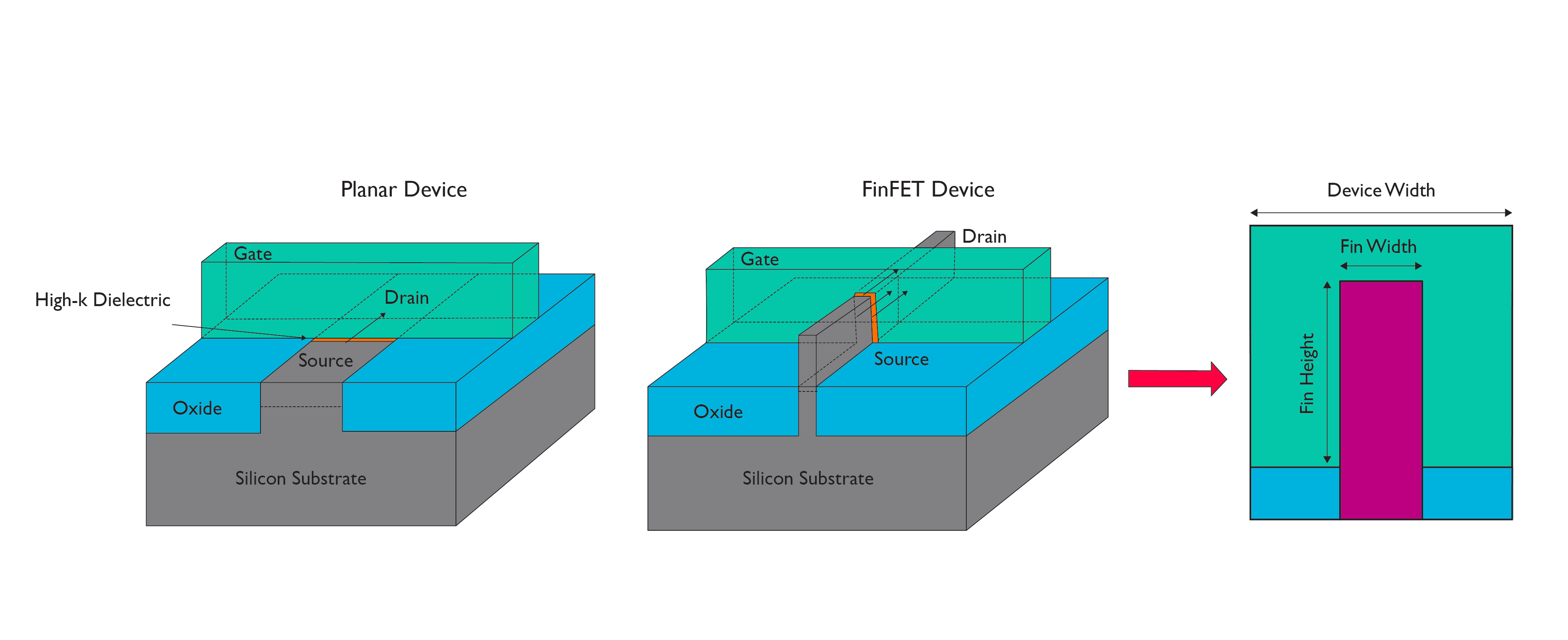
With advanced geometry planar FET technologies, such as 20nm, the source and the drain encroach into the channel, making it easier for leakage current to flow between them and making it very difficult to turn the transistor off completely (see fig 1a). FinFETs are 3d structures that rise above the substrate and resemble a fin, hence the name. The 'fins' form the source and drain, effectively providing more volume than a planar transistor for the same area (see fig 1). The gate wraps around the fin, providing better control of the channel and allowing very little current to leak through the body when the device is in the 'off' state. This, in turn, enables the use of lower threshold voltages and results in better performance and power.


Many semiconductor design companies are moving rapidly to manufacturing their devices on the advanced 16nm and 14nm FinFET based process geometries, simply because the performance and power benefits are compelling. Many test chips have taped out and the results are now starting to come in.

One of the earliest manufacturing providers at the 14nm process node, Samsung has been developing FinFET process technology for several years and is now ready for early adopter production. Samsung's 14nm LPE process is providing almost 150% better performance from a die half the size of the previous node and improving power consumption by around 150% when compared to its 28nm process technology (see fig 2).


From the economic perspective, data from International Business Strategies shows that the move to 20nm and FinFET results in essentially the same cost per die (Q1 2014 estimates), especially as devices increase in size (see fig 3).


FinFET devices can operate from a lower supply voltage than planar transistors since they have a lower threshold voltage. This drop in supply voltage can improve dynamic power consumption significantly: at the least, users can expect a 20% improvement from a drop in supply voltage of just 0.1V and this constitutes a strong driver for FinFET adoption.

Given that the transistors can operate at a much lower voltage than nominal, additional dynamic power savings on that facet alone would be achievable. In addition, foundation library providers are investigating whether or not it makes sense to introduce smaller height standard cells that could reduce dynamic power consumption further.

These providers are likely to release different height libraries, allowing designers to target specific performance or power applications as foundry process design kits are stabilising for production.

FinFET processes are already in production. Intel was one of the first semiconductor manufacturers to use the 22nm node, where it reported power savings of up to 50% when compared to its 32nm process. Semiconductor manufacturers such as TSMC, Samsung Foundry and GlobalFoundries are also moving to production rapidly with several test chips already taped out. But what does it take to move a design to the new FinFET processes and take advantage of the performance and power benefits?

The 20nm process node was necessary to help build the foundation for the advanced FinFET processes. With the smaller device geometries, traditional lithography/optical manufacturing techniques no longer have the required resolution where double patterning – using litho-etch-litho processing – becomes necessary. The number of manufacturing design rules has increased significantly and these have to be handled by various eda tools, such as place and route, physical verification and extraction.

The industry's experience with 20nm has paved the way for an easier transition to FinFET processes. Many of the tool improvements can still be applied, but the handling of FinFETs does require a few more changes; for example, SPICE BSIM-CMG models had to be created to add the 3d effects. It is also true that, with 3d transistors, capacitance becomes a primary concern. EDA tools must build in high resistance interconnect optimisation in order to mitigate these capacitive effects. Layer awareness is also essential to provide optimal metal layer assignment during routing of the design.

Although FinFET processes may seem new, development of the technology itself has been in progress for almost a decade. The industry has worked together to make the shift to an advanced new process node as seamless as possible, with minimal impact to current design methodologies.

Consumer appetite for new functionality remains high and the move to designing with FinFET process technologies will help fill that need and keep Moore's Law very much alive.

Mary Ann White is product marketing director, Galaxy Implementation Platform, for Synopsys.

Thursday, 30 October 2014

Intel's Broadwell processor revealed

Intel's Broadwell processor revealed


The 14-nm Core M aims to upend the tablet market


INTEL HASN'T TAKEN TOO kindly to the revolution in mobile devices that has happened largely without its participation. The rise of smartphones and tablets with ARM-compatible chips onboard has become a major threat to Intel's dominance in the processor business—and this is, after all, a company built on the mantra that "only the paranoid survive."
Thus, for several technology generations, Intel has slowly adjusted its heading to better compete in mobile devices. The firm has used its expertise in chip manufacturing and design to cram PC-like performance into ever smaller footprints. Last year's Haswell chip brought huge progress in terms of power consumption, battery life, and system sizes. This year, a new processor code-named Broadwell promises dramatic gains once again, thanks in part to the world-class nanoscale technology in Intel's 14-nm chip fabrication process.
The first Broadwell-based processors will carry a new brand name, Core M, and they will target very small systems indeed: iPad-like tablets that are less than nine millimeters thick and have no fans to cool them. Fitting a PC-class processor into such a device is no easy task. Intel claims to have achieved this feat by tweaking nearly every part of the Broadwell silicon and surrounding platform in order to reduce its size and power consumption. More impressively, they say they've kept performance steady at the same time.
Enforcing Moore's Law: Intel's 14-nm process
One key ingredient in Broadwell's success is Intel's 14-nm manufacturing process, the world's first of its kind. Broadwell has been very publicly delayed due to some teething problems with this new process. In a briefing last week, however, Intel VP and Director of 14-nm Technology Development Sanjay Natarajan told us that the 14-nm process is now qualified and in volume production.
In fact, Natarajan shared quite a few specifics about the 14-nm process in order to underscore Intel's success. His core message: the 14-nm process provides true scaling from the prior 22-nm node, with virtually all of the traditional benefits of Moore's Law intact.
Moore's Law has made the massive advances in microelectronics over the past 40 years possible. Its basic formulation says that the number of transistors one can pack into a given area of a chip will roughly double every couple of years. Intel has moved mountains to keep Moore's Law on track, and it has reaped huge benefits for doing so. The rest of the semiconductor industry has followed the same path, but in recent years, it has done so from a fair distance behind Intel. For instance, this 14-nm process is the second generation to employ what Intel calls tri-gate transistors (which the rest of the industry calls FinFETs). Other firms have yet to ship first-generation FinFET silicon.
Shrinking on-chip features to ever-smaller dimensions is an incredibly difficult problem, and the complexity of the task has grown with each successive generation. When questioned during a press briefing we attended, Natarajan was quick to admit that the familiar naming convention we use to denote manufacturing processes is mostly just branding. The size of various on-chip elements diverged from the process name years ago, perhaps around the 90-nm node. That said, Intel Fellow and process development guru Mark Bohr quickly pointed out that transistor densities have continued to scale as expected from one generation to the next. In other words, Moore's Law is alive and well.
Source: Intel.
To illustrate, Natarajan showed how the fins comprising Intel's tri-grate transistors have grown closer together at the 14-nm node—fin pitch has been reduced from 60 to 42 nm—while the fins themselves have grown taller and thinner. The closer placement improves density, while the new fin structure allows for increased drive current and thus better performance. This higher performance, in turn, allows Intel to use fewer fins for some on-chip structures, further increasing the effective density of the process. Fewer fins also means lower capacitance and more power-efficient operation.
Source: Intel.
The gate pitch has been reduced from 90 to 70 nm and, as shown above, the spacing of the smallest interconnects has dropped even more dramatically, from 80 to 52 nm.
Source: Intel.
The cumulative result of these changes is perhaps best demonstrated by looking at a fairly common benchmark: the size of a six-transistor SRAM cell. On Intel's 22-nm process, a 6T cell occupies 0.108 square micrometers of space. The same structure at 14-nm takes up only 0.0588 square micrometers—or 54% of the area required at 22-nm. That's classic Moore's Law-style area scaling.
Source: Intel.
The benefits of the 14-nm process extend beyond sheer density. Natarajan shared the graph above to convey the power and performance advances offered by this 14-nm process. Essentially, it can flip bits at higher speeds than prior generations while losing less power in the form of leakage along the way. Intel can choose to tune its products for different points along the leakage-performance curve shown above, but in each case, chips built on the 14-nm process should offer a nicer set of tradeoffs than those from prior process generations.
This next illustration is perhaps the most telling, because it addresses one of the key threats to Moore's Law going forward: economics. I said before that the transition to each smaller process node has been more difficult than the last. Chipmakers have had to use ever more exotic techniques like double-patterning—creating two separate masks for photolithography and exposing them at a slight offset—in order to achieve higher densities. Doing so increases costs, and as a result, one of the key corollaries of Moore's Law has been threatened. If moving to finer process nodes can't reduce the cost per transistor, the march of ever-more-complex microelectronics could slow down considerably. Some chipmakers have hinted that we'll be approaching that point very soon.
Source: Intel.
By contrast, Intel says the math continues to work well for its process tech. The area per transistor is dropping steadily over time, while the cost for each square millimeter of silicon is rising at a slower pace. The net result remains a steady decrease in cost per transistor through the 14-nm node. In fact, Bohr told us that he expects Intel to deliver an even lower cost per transistor in its upcoming 10-nm process.
Despite the delays, then, Intel is bullish about its process tech advancements and confident that its 14-nm technology is ready to roll. Natarajan says the company is now shipping 14-nm production chips to its customers, and the first Core M-based products should arrive on store shelves in time for this year's holiday season. Two fabs, one in Oregon and the other in Arizona, are slated to be producing 14-nm wafers this year, with another plant in Ireland scheduled to ramp up production in 2015. Natarajan expects sufficient 14-nm silicon yields and wafer volumes to support "multiple 14-nm product ramps in the first half of 2015."


SEMICON Update: FinFet

SEMICON Update: 450mm, EUV, FinFET, and More

I spent all of last week at SEMICON West meeting with customers, potential customers, partners and various industry analysts and experts. I was involved in many interesting discussions over the course of the week and I thought I would share some of the more interesting observations:

Alternate Fin Materials Pushed Out
I have for some time been expecting that Intel would introduce Germanium (Ge) fins for PMOS at 14nm. Furthermore I had seen an announcement from TSMC that they would be introducing Ge fins at 10nm. My view was Intel would be the first adopter for Ge fins at 14nm and then the usage would become more widespread at 10nm. I furthermore expected we might see Indium Gallium Arsenide (InGaAs) fins for NMOS first use at 10nm and wide spread use at 7nm. What I am now hearing is that Intel has abandoned Ge fins for 14nm and TSMC has pushed them out to 7nm. It looks like adoption of Ge has been pushed out one node industry wide and presumably InGaAs will also be pushed out at least one node. Furthermore, what I am hearing is that Intel’s 14nm process is now a shrink of the 22nm process with no new technology introductions. I am also hearing Intel is still struggling with 14nm yields but they are ramping up anyway and working on yield as they go. Running volume can be a very effective way to make rapid progress on yield if you can afford the scrap.

450mm Still Delayed
After SPIE earlier this year I reported that 450mm was delayed until after 2020. Everything I heard at Semicon was consistent with this. My sense is that Intel and TSMC in particular have both backed off on their timing.

EUV Delays
The continued delays in EUV are making insertion at 10nm less and less likely. Insertion at 7nm will either require a high NA tool or multi-patterning. Higher NA has a whole set of problems of its own to add to the current problem list. Meanwhile companies continue to cost reduce and prefect multi patterning.

28nm A Long Lived Node?
There have been a number of comments in the media about 28nm being a long lived node. I would just like to point out that all foundry nodes tend to be long lived. You can still get 500nm, 350nm, 250nm, 180nm, 130nm, 90nm, 65nm and 40nm nodes from TSMC, UMC and many others. In fact it wasn’t that long ago that I was hearing that 65nm was still the sweet spot for most designs, it might still be true. I think the real point people are trying to make is that 28nm will continue at higher than normal levels longer than normal because of a perceived lack of value at 20nm and below. I will discuss this more in the next two sections.

20nm Is Ramping at TSMC
Morris Chang has stated he expects 20nm to be the fasting ramping node in TSMC history. There are reports coming out that Qualcomm and Apple both have 20nm designs running at TSMC (Chipworks just announced an analysis of a 20nm Qualcomm part presumably purchased on the open market). It is pretty clear 20nm is going to be a big node at TSMC, I think the more interesting question is will 20nm take off anywhere else.

Scaling and cost
There have been a number of reports that cost reductions will end at 28nm and that at 20nm and 14nm cost per transistor will rise. Historically each new node has resulted in an increase in wafer cost but at the same time an even greater rise in transistor density has yielded a cost per transistor reduction. I had been planning to write an article on this and I still might, but I thought I would share some observations here.

At 20nm extensive multi-pattering is required driving up wafer cost more than “normal” versus the 28nm node, however, TSMC is reporting a 2X increase in transistor density for 20nm versus 28nm. 20nm wafer costs are not 2x 28nm wafer costs and cost per transistor should therefore go down although less than “normal” and I am in fact hearing that early adopters at TSMC are seeing reductions in cost per transistor.

This brings us to 14nm (or 16nm as TSMC calls it). 14nm is a very interesting node for several reasons. First of all it is the first FinFET node for most logic producers. Secondly, the major foundries have all decided to use the same backend for 14nm that they used for 20nm suggesting little or no increase in transistor density will result. There have been some projections of major increases in wafer cost at 14nm due to “FinFET and Multi-pattering”. Since most logic multi-pattering is in the backend and the backend isn’t shrinking I wouldn’t expect multi-pattering to drive a lot of additional cost versus 20nm. Also, FinFETs actually have simpler processes than bulk planar (less mask layers although some steps are very difficult) so I am not expecting an unusually large cost per wafer increase for 14nm versus 20nm. In terms of transistor density I am hearing there will be about a 5% to 10% improvement. The net result is I would expect cost per transistor to be relatively flat to slightly up at 14nm. What I am hearing is cost per transistor will actually go down, but only slightly.

At 10nm all the foundries are expected to do a full shrink. 10nm will require more complex multi-pattering schemes and I expect that the density improvement will result in a reduction in cost per transistor, although likely smaller than the “normal” trend.

200mm Growing Again
SEMI presented a very interesting data point that 200mm wafer volumes have gone up this year. Typically at this point in the life cycle of an older wafer size it would be in a slow steady decline and yet 200mm has grown recently. On top of this, presentations discussing “The Internet Of Things” all seem to include a discussion of all the additional 200mm fabs that will be needed to make the sensors. 300mm represents the majority of silicon wafer area run by the semiconductor industry today and is rapidly growing, 150mm and smaller wafer sizes are all declining but it looks like 200mm will also see some growth for at least the next few years. It will be interesting to see how this all plays out if 450mm is ever introduced. 450mm could result in a lot of low cost 300mm surplus hitting the market that might drive applications to jump from 200mm and smaller wafer sizes to 300mm. Low cost - used 300mm equipment and fabs have already led to the TI 300mm analog Fab and Infineon 300mm discrete fab.

3D NAND
There was a very interesting tech spot on 3D NAND run by Mike Corbett of Linx Consulting. Samsung presented on the market, Applied Materials on Deposition Challenges, Tokyo Electron on Etching Challenges and Mark Thirsk of Linx on materials and cost. 3D NAND appears positioned to provide a future scaling path for NAND with much better performance and eventually better cost. To-date 3D NAND is going into high-end applications (less cost sensitive) but with the introduction of a 32 layer devices later this year wider usage is expected. During the question and answer part of the session one person commented that the 3D cell sizes are a lot bigger than people realize. If you do the math he is correct, I get something like 26F2 as the effective cell size based on the size of the arrays. When you take into account 24 layers and 2 bits per cell, the area per bit is larger than current 16nm 2D NAND. However, when you get to 32 layers the area per bit is smaller and additional layers only increase the lead. 3D NAND continues Moore’s law and scaling by going into the third dimension. This is a technology to watch and it will be interesting to see if analogous solutions can be developed for DRAM and even logic.

The Shrinking Show Floor
Several years ago I had a booth at SEMICON West but I didn’t find the cost benefit trade-offs to be favorable. The last couple of years I have foregone a booth and just attended the show setting up meetings to take advantage of so many people I wanted to meet with all being in the same place at the same time. Walking the show floor this year it struck me as smaller than in the past. I have the impression that more and more companies are forgoing a booth on the show floor for off-site meeting space in surrounding hotels. If this is in fact an accurate view of what is happening this strikes me as a bad trend for SEMI and the show since they presumably get no revenue from off-site meetings.

ARM describes finfets

ARM describes finfets in the real-world


Finfet technology, with its 3D structure, is seen as the key semiconductor technology for the next generation of deep sub-micron chip design. Leah Schuth describes how physical IP developers will rise to the challenge.
The semiconductor industry faces a major change in the way that ICs are made in order to keep improving performance and density – a change that has potential ramifications for design methodologies. Foundries are preparing to ramp up 14nm and 16nm processes that use three-dimensional transistor structures based on the finfet concept as they provide higher performance than can be achieved using the planar transistors of the 20nm generation.
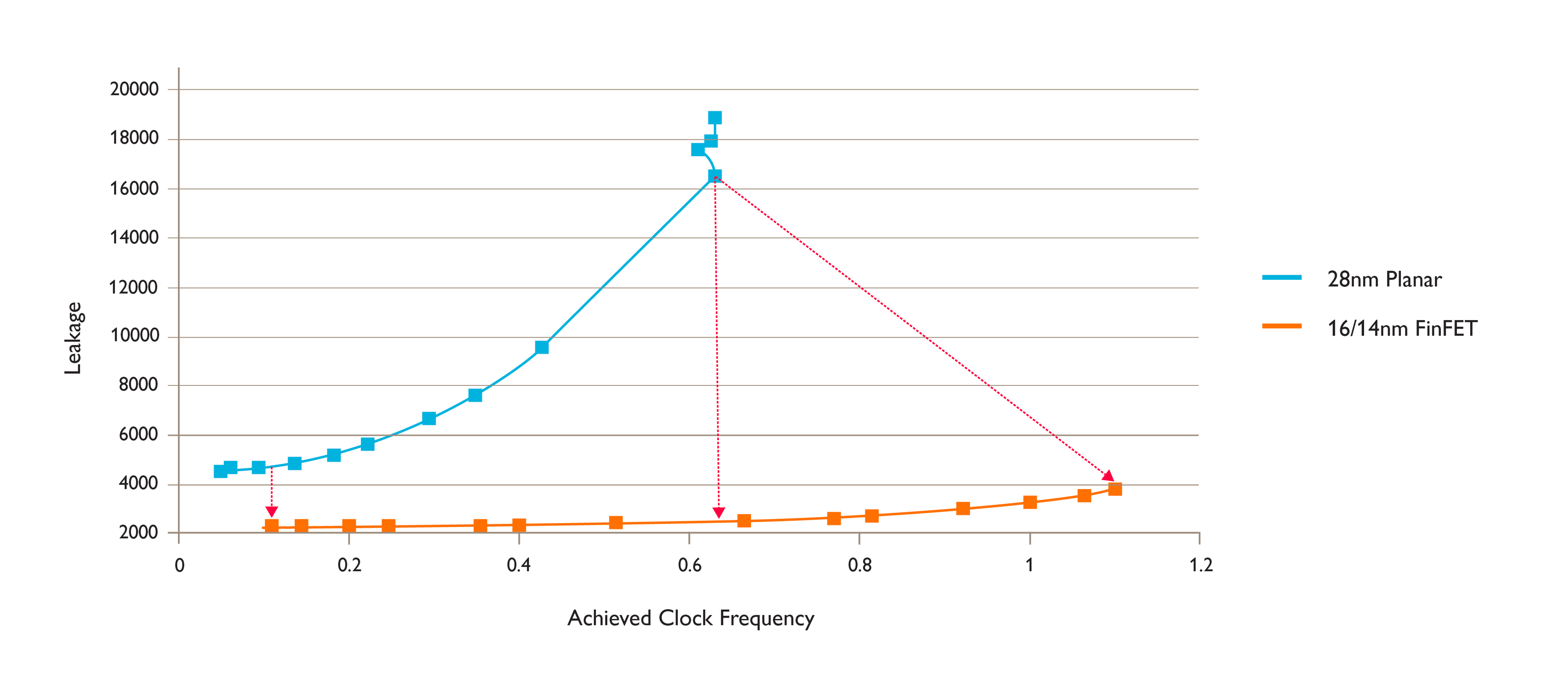
Raising the channel through which carriers flow so that the gate can be wrapped around three of its sides means the gate then exhibits much greater electrostatic control. This overcomes the short-channel effects that lead to excessive leakage and other problems of nanometre-scale planar transistors fabricated on bulk-silicon wafers.

 ARMfig1
Figure 1: Graph to illustrate better Leakage Control Across Frequency Range

A further advantage of the multi-sided gate is more drive current per unit area than planar devices – the height of the fin can be used to create a channel with a larger effective volume than a planar device with the same equivalent gate length. This translates into better effective performance.
The added performance capability of finfets can be used to achieve higher frequency numbers compared to bulk for a given power budget. The power reduction can come from two sources: reduced need for wide, high-drive standard cells; and the ability to operate with a lower supply voltage for a given amount of leakage. But changes to design techniques will be needed to enable this performance to be fully realised.
Standard cell-based flows remain key to high-productivity IC implementation. The cell abstraction has underpinned the synthesis-driven flow for several decades, providing the basis for highly automated digital circuit implementation that allows comparatively small teams to manage multi-million gate designs. Changes to the transistor structure and their associated layout-dependent effects threaten to break through the clean interfaces between the physical, cell and logical layers of the design process, forcing designers to take into account low-level features when laying out circuitry. However, by bringing more intelligence to the cell level, it is possible to maintain the productivity advantages of the standard cell abstraction and still tease out the power, performance and area (PPA) advantages promised by finfet-based processes.
The finfet brings with it some fundamental changes to circuit structure that are driven by its physical form (Figure 2).The fins on a given process have a fixed width and pitch. In contrast to planar processes where transistors can be made wider by arbitrary amounts to improve their overall drive strength and to improve their performance with large fanouts or high-capacitance buses, a finfet’s effective width can only be changed by adding more fins to the transistor. As well as increasing the complexity of analogue and custom circuit design, fin quantisation has subtle but important ramifications for digital circuit implementation.
In general, finfet-based processes benefit from as narrow a fin pitch as possible as this provides better density, flexibility and performance. The processes used to create the fins rely on chemical self-alignment techniques that can yield pitches 25 per cent smaller than the pitch of lines on the finest layers of metal interconnect, M1 and M2. These metal layers are currently drawn using two independent masks that are overlaid into one composite exposure rather than using self-aligned processes. The minimum pitch of these metal layers is determined by the overlay error, resulting in a higher pitch than can be achieved for the self-aligned fin-formation steps.
The mismatch in fin and M2 pitch – which conventionally runs parallel to the fins – needs to be factored into the design of standard cells used to implement the bulk of the digital logic that will be used in a finfet-based IC.
 armfig2
Figure 2: Finfet vs Planar
In the case of finfet -based processes, there are only a few valid ‘gear ratios’ between fin and metal pitches that can result in viable standard-cell libraries, which need to be designed to fit each of their cells into a fixed number of tracks. Even then, some combinations will result in inflexible metal grids that make it difficult to carry sufficient current to cells on critical paths. Nanometre processes are increasingly prone to effects such as electromigration that will reduce the lifetime of the IC by gradually thinning out wires subject to high currents until they break.
For maximum metal wiring density, double-patterning rules enforce not only the pitch of metal traces but their width. As a result is not always possible to draw wider metal traces to carry the large currents needed for cells that provide a high drive. Some ratios of fin count to metal trace count do allow for more flexible use of metal interconnect for power routing.
These enable the use of wider, more resilient power rails where they are needed, alongside tracks of cells able to trade higher logic routing density for power delivery. To be able to take advantage of these structures calls for a much deeper understanding of standard-cell architecture than is usually the case in conventional place-and-route tools, which are designed to treat standard cells as black boxes with a set of I/O and power pins in predetermined locations.
Tools that are able to use their understanding of the internal standard-cell architecture and remap cells according to the needs of the logic can provide the additional flexibility required to make full use of these new structures without demanding a thorough retooling of the IC-implementation flow. The same understanding can aid other parts of the flow, through to late changes in design that result in engineering change orders (ECO).
Because design rules are more restrictive than in the past, implementing ECOs has become more difficult to perform as even a small change can lead to issues with mask colouring on double-patterned layers. A flow that incorporates tools able to comprehend the local standard-cell environment can manipulate the design at a deeper level to allow ECOs to be implemented as transparently as possible.
Greater understanding of the internal architecture of standard cells will help with other issues raised by the migration to nanometre processes based on finfets. As designers attempt to take advantage of the higher performance of the 3D transistors and push up clock speeds, they will encounter tougher variability challenges. Although finfets demonstrate lower variation than planar transistors for some key metrics, variability remains a major obstacle to timing signoff and is exhibited in a number of ways that cross the boundary between standard cells and the routing layer.
Traditionally, such variations would be incorporated into guard bands that limit clock speed, limiting the performance gains that can be achieved with the finfet structure. Better analysis and correction techniques can recover much of this performance loss, leading to higher clock speeds and products that are more competitive in the market.
The double-patterning techniques employed in the 14nm and 16nm generation of finfet -based processes have been shown to lead to significant variations in path delay. For example, a small shift in the alignment of one of the two masks used to image the interconnect patterns can increase the coupling capacitance between the gate electrode and the wiring, leading to an increase in path delay.
Because the shift will be consistent across the entire mask, the delay for transistors linked by the pattern on that mask will be correlated – something that can be taken into account by more advanced analysis tools that have an understanding of the behaviour and internal connections of each standard cell. By taking these correlations into account and taking corrective measures, the pessimism introduced by coupling capacitance variation can be removed and target clock speeds increased.
Interconnect parasitics, particularly the high resistance of metal traces in finfet-based processes, also limit the performance of clock tree, which use a large number of long-distance connections to provide consistent timing across the IC. Traditional techniques such as buffer insertion increase power consumption. By employing knowledge about the underlying standard cells it is possible to perform more intelligent clock-tree optimisation and provide low-skew timing signals without eating into the power budget.
The decrease in device geometries is also leading to increases in the probability of single-event upsets caused by ionising radiation that lead to incorrect results and system crashes. Analysis of the structure of cells in their circuit context, potentially replacing them with hardened versions, can reduce the probability of improper behaviour in the event of alpha particles.
The move to finfet-based processes brings about a number of process-level changes that have ramifications for digital design that if not addressed can lead to poor IC performance. Although these physical effects potentially threaten the highly stable standard cell-based flow, the introduction of tools to address SoC design at the cell level will help maintain the stability of the flow and enable the full performance of finFET-based processes to be realised.


Writer is Leah Schuth, manager technical marketing, physical design at ARM
- See more at: http://www.electronicsweekly.com/news/research/process-rd/arm-describes-finfets-real-world-2014-10/#sthash.0dfMrbzd.dpuf


FinFETS Fabs

GlobalFoundries licenses Samsung process tech, grants AMD access to FinFETs


 — 12:27 PM on April 17, 2014
As you may know, AMD's former manufacturing arm is now a part of GlobalFoundries, which manufactures chips on contract for multiple customers while remaining the source for AMD's highest-performance CPUs. Like AMD before it, GlobalFoundries is part of the Common Platform Alliance along with Samsung and IBM. The three firms share R&D costs and implement similar techniques for building chips.
Today, the relationship between a couple of those partners shifted fundamentally when GlobalFoundries announced that it has licensed Samsung's process technology.
The tech being licensed is the next major step forward, a 14-nm process that uses a new transistor structure known as FinFETs or, as Intel calls them, tri-gate transistors. Intel made the transition to FinFETs at its 22-nm process node and saw some fairly dramatic benefits in terms of switching speed and power efficiency (which are often two sides of the same coin in process tech discussions). Other firms in the industry have struggled to reap the usual power and speed benefits when moving below 28-nm process geometries without FinFETs. Most of these firms have scheduled FinFETs for the 16- or 14-nm nodes, with several delays. Meanwhile, even Intel has delayed its 14-nm process due to technical difficulties.
Samsung appears to have succeeded in developing a capable 14-nm FinFET process. Here's how the press release describes the technology being licensed:
Developed by Samsung and licensed to GLOBALFOUNDRIES, the 14nm FinFET process is based on a technology platform that has already gained traction as the leading choice for high-volume, power-efficient system-on-chip (SoC) designs. The platform taps the benefits of three-dimensional, fully depleted FinFET transistors to overcome the limitations of planar transistor technology, enabling up to 20 percent higher speed, 35 percent less power and 15 percent area scaling over industry 20nm planar technology.
At last year's Common Platform Technology Forum, GlobalFoundries shared its own roadmap for 14-nm process technology. During that same event, the Alliance members admitted that their manufacturing methods were diverging since their customers preferred customization over fab-to-fab portability.
Today's news, then, marks a change in direction. GlobalFoundries will so closely implement Samsung's technology that the two partners are once again talking about portability between fabs:
Through a proven level of fab synchronization never previously achieved outside of a single company, Samsung and GLOBALFOUNDRIES will use a coordinated copy-smart approach involving materials, process recipes, integration and tools. The company will also run fab-sync test chips on a regular basis to ensure that the fabs are the 14nm FinFET process exactly the same.
GlobalFoundries confirms that this news means the end of the road for its own 14XM process. The firm says Samsung's process tech has two key advantages over 14XM. Samsung's tech is further along in development, so the schedule is more attractive, and Samsung's 14-nm FinFET tech provides better area scaling by cramming more gates into a given area.
This licensing arrangement instantly makes the chip foundry business quite a bit more interesting. Samsung famously manufactures SoCs for its biggest rival and a huge customer: Apple. Now, some or all of Apple's production could move to GlobalFoundries fairly easily, assuming something else (like a rumored move to TSMC) doesn't change the picture entirely.
Perhaps the biggest beneficiary of this licensing deal will be AMD, who gains access to a capable 14-nm FinFET tech for the production of its future CPUs and SOCs. AMD's Kaveri APUs actually ran slower than their predecessors after transitioning from GloFo's 32-nm SOI process to 28-nm bulk silicon. Meanwhile, AMD competes most directly with the process tech leader, Intel.
AMD veep Lisa Su provided an appropriately vague-but-positive statement for the press release announcing the deal:
"This unprecedented collaboration will result in a global capacity footprint for 14nm FinFET technology that provides AMD with enhanced capabilities to bring our innovative IP into silicon on leading-edge technologies," said Lisa Su, senior vice president and general manager of Global Business Units at AMD. "The work that GLOBALFOUNDRIES and Samsung are doing together will help AMD deliver our next generation of groundbreaking products with new levels of processing and graphics capabilities to devices ranging from low-power mobile devices, to next-generation dense servers to high-performance embedded solutions."
If in fact AMD has some capable new CPU architectures in the works, the availability of a solid 14-nm FinFET process could be the final piece needed to restore the firm to competitiveness with Intel.

Race to the FinFETS

The demand for smartphones and tablets with better performance and longer battery life has been driving the industry to come up with chips that are faster, smaller and use less power. To remain on this treadmill known as Moore’s Law, chipmakers have in recent years relied on a series of technological breakthroughs, most recently 3-D transistors known as FinFETs.
Intel started production with FinFETs in late 2011 with its 22nm Ivy Bridge processors and since then it has shipped more than 500 million chips. These are mostly for PCs and servers, though it is on target to ship 40 million tablet processors this year, and it is offering the technology to other customers as a foundry. Now the other foundries, which manufacture chips for customers such as Apple, Qualcomm, Samsung and MediaTek, are scrambling to catch up.
In the past week TSMC, the world’s largest contract chipmaker, has made two announcements meant to signal its progress on FinFETs. First, TSMC said it had produced a working network processor, with 32 ARM Cortex-A57 CPU cores, for HiSilicon, the chip division of Huawei. Then, earlier this week, the foundry announced that a 64-bit ARM big.LITTLE test chip manufactured on its 16nm FinFET process delivers sustained speeds of 2.3GHz with its big Cortex-A57 cores and uses only 75 milliwatts of power with its little A53 cores on typical applications.

FinFET 14nm Strategies

Intel and IBM to lay out 14nm FinFET strategies on competing substrates at IEDM 2014

The development of increasingly sophisticated and energy-efficient CMOS technology for mobile, client and cloud computing depends on a continuing stream of advances in the process technologies with which the complex integrated circuits are built. Among the most promising chip technologies are transistors calledFinFETs, which have attracted significant R&D investment and have begun to appear in commercial products.
But the technology is complex and the path forward isn’t settled, and in two late-news papers to be given at this December’s IEEE International Electron Devices Meeting (IEDM), Intel and IBM will present dueling approaches to the development of FinFET technology for the 14nm technology node, the semiconductor industry’s next big hurdle.
The IEDM is the forum where top technical experts in micro- and nanoelectronics gather to disclose, discuss and debate breakthrough technologies in the field. The 60th annual IEDM will be held at the Hilton San Francisco Union Square Hotel from December 15-17, 2014, preceded by day-long short courses on Sunday, Dec. 14 and a program of 90-minute tutorials on Saturday, Dec. 13.
All modern transistors have a channel to conduct electricity and one or more gates to turn the current on and off. FinFETs have long, thin fin-like channels (hence the name) surrounded by multiple gates. This design leads to greater performance and enhanced energy efficiency. Both Intel and IBM will present fully integrated14nm FinFET technologies at the IEDM.
Intel, which began using FinFET transistors commercially in its “Ivy Bridge” and “Haswell” processors at the 22nm node, will detail the second generation of that technology.[i] Made on a standard bulk silicon substrate, the new “Broadwell” 14nm technology has been released commercially and is in production as part of Intel’s latest family of microprocessors.
Among the technical features Intel will discuss at the IEDM are: a novel doping technique to prevent current leakage under the fins and to maintain very low doped fins, resulting in improvement in variation; two levels of air-gap-insulated interconnects (electrical connections) at ultra-narrow 80 and 160nm minimum pitches, yielding a 17% reduction in capacitance delays; eight layers of 52nm pitch interconnects embedded in low-k dielectrics; an embedded 140Mb SRAM memory with a tiny cell size of 0.0588µm2; and saturated drive currents significantly higher than for Intel’s 22nm first-generation FinFETs (improvements of 15% and 41% for NMOS and PMOS transistors, respectively). The transistors operate with a supply voltage of only 0.7 Volts.
The researchers also will discuss how aggressive design rules enabled the production of very high aspect ratio rectangular fins (8nm wide and 42nm high) at unprecedented levels of uniformity.
IBM, meanwhile, will describe a very different approach to 14nm FinFET transistors.[ii] The IBM devices are made not from a standard bulk silicon substrate but from an insulating substrate known as SOI, a more expensive material but one which simplifies manufacturing in terms of device isolation. These devices are more than 35% faster than IBM’s 22nm planar (i.e. standard, non-FinFET) transistors, with an operating voltage of just 0.8 volts.
The IBM technology features what may be the smallest, densest embedded DRAM memory ever demonstrated (a cell size of just 0.0174µm2) for high-speed performance in a fully integrated process flow. IBM also designed an elegant way to make the technology suitable for both low-power and high-speed applications, using a unique dual-workfunction process that optimizes the threshold voltages of both NMOS and PMOS transistors without any mobility degradation in the channel.
Because the technology is envisioned for use in system-on-a-chip (SoC) applications ranging from video game consoles to enterprise-level corporate data centers, the IBM design also features a record 15 levels of copper interconnect to give circuit designers more freedom that ever before to distribute power and clock signals efficiently across an entire SoC chip, which may be as large as 600mm2.
Making transistors smaller, or scaling them according to Moore’s Law, is what has traditionally driven exponential progress in nanoelectronics and information technology. With today’s nanoscale-sized devices that has become difficult and expensive, which is why new transistor architectures such as FinFETs have become so appealing.

VIDEOS ON FINFET

Introduction to 3D Finfets.

http://synopsys1.http.internapcdn.net/synopsys1/svsnug2012-chenming-keynote/main.htm#

Understanding The FinFet Semiconductor Process

https://www.youtube.com/watch?v=Jctk0DI7YP8


https://www.youtube.com/watch?v=6LcTrp6SB3o